Learning Kicad
A couple of weeks ago I decided that I wanted to learn a bit about PCB design. I’ve only ever designed one PCB before, a couple of years ago when I was trying to make a set of capacitive touch paddles for morse code. That wasn’t a terrifically complicated project, the routing wasn’t difficult, and it was truly single sided (no vias or nothing). I’ve always wanted to design more PCBs so I figured now would be a good time to give it a shot.
The obvious question is: what to make? I needed a circuit to build a PCB for, and I was more interested in learning the process of PCB development right now, so undertaking a whole project just to eventually get to design a PCB at the end didn’t seem like a great option. One weekend last year I made a little LED spinner project using a PIC12F629 microcontroller and a couple of shift registers, and that seemed like a fine project to make into a board, so I decided to start with that.
My previous experience with PCB design was with Eagle. Eagle is fine for what it is, but it is closed source, there is some monitezation there, and most of the research that I was doing right now suggested that it was no longer the popular way of doing things. The popular things now seemed to be Altium Designer and KiCad. KiCad is open source, pretty featureful, runs on Linux, and I found a lot of tutorials for it, so I decided to go with KiCad.
I won’t talk too much about the learning process itself, since it’s mostly just watching tutorials, fumbling through menues, and rote repitition, but I did want to mention the Phil’s Lab YouTube Channel. Phil makes a ton of very interesting PCB related content, has entire tutorials for KiCad and Altium Designer (that I relied on heavily), and is honestly just a ton of fun to watch if you’re into this kind of thing.
I decided that I wanted to make a two layer board (for such a simple design more layers seemed wasteful, though it would’ve been handy during routing). I also wanted to do most everything in SMD (except for the LEDs, I used standard 3mm THT LEDs since I have a billion of them). I also had a particular form factor in mind. I wanted it circular, and I wanted it to have a radius of 61mm to fit into a particular container that I have a lot of laying around.
The basic steps of making a PCB are pretty straight forward:
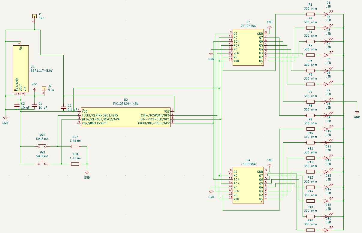
- In the schematic editor, make your schematic. You must include EVERYTHING in your schematic, even things that don’t seem electrically pertinent (eg mounting holes if you plan on mounting the board with screws, pin terminals, etc).
- Once your schematic is squared away (there is a schematic design rule check function you can check with), you need to assign footprints to your components. For every component utilized in your design, you need to assign a physical footprint to associate to the part.
- Once all footprints are assigned and the DRC passed, switch over to the PCB editor and import your schematic. This copies each of the footprints from the schematic over to the PCB, and it will include thin lines that indicate how components should be connected to each other.
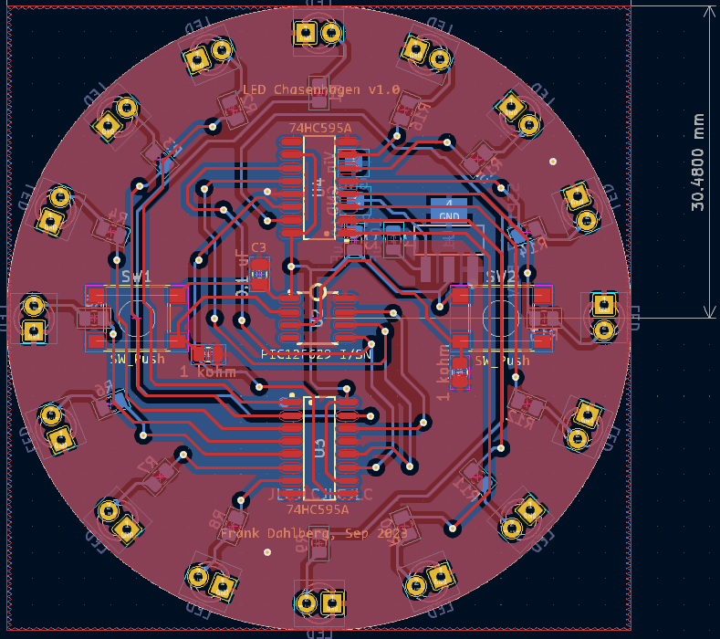
- Arrange the components as you’d like. You can make your edge cuts to specify the board geometry first, or if you’re not design constrained against board geomerty then just lay everything out the way you want first.
- On the edge cut layer, lay out the edge cuts for the board. This sets the geometry and size of the PCB itself.
- Begin routing. This is the biggest step by far. Each and every component needs to be connected as specified in the schematic. This is where more layers becomes helpful. Since this is a PCB two traces cannot intersect on the same layer, so it becomes a layout game of connecting everything properly without running out of space. This was a very simple PCB, so I wasn’t overly concerned with trace length, signal type, etc, but for more complicated high power, high speed, mixed signal, etc boards it becomes important to have fixed length routes, not route analog and digital signals near each other, the trace width and separation can change for high voltage stuff, etc.
- Set the fills. You can fill areas of the board with a ‘pour’ to ease routing. For example, it’s normal to have at least one ground plane in any design where you just fill an area with ground, and then anything needing a path to ground can just find the closest fill point.
- Arrange your silkscreen. Once the layout, routing, and fill is done, you set your silkscreen to have any text data, art, documentation, etc needed to ease assembly and use.
- Make gerbers and send to fab. This is the best part! Once the design is done, export the design to layer and drill gerber files, zip them up, upload them to a gerber viewer to view the layout, and send them to the fab for production.
There are several more steps for more involved boards, but for a simple board like this that is pretty much the process. Notably, for multilayered boards that have more then two layers you have to be concerned about the board ‘stackup’. This is determining what each layer performs, and how those layers may interfere which each other. For example, if you have a signal layer sitting directly on top of another signal layer you may get cross talk and interference between the layers, so it’s common to have a GND-SIGNAL-VCC-SIGNAL-GND stackup for some five layer boards. There’s lots of theories, board stackup is a whole topic in itself. For this two layer board I just had each side be a ground plane, and also both sides carried signals where necessary (normal for a two layer board). I’ve included photos of the schematic and PCB design in KiCad below (NOTE: there are some considerable bugs in the pictures below that I left in for the screenshot).
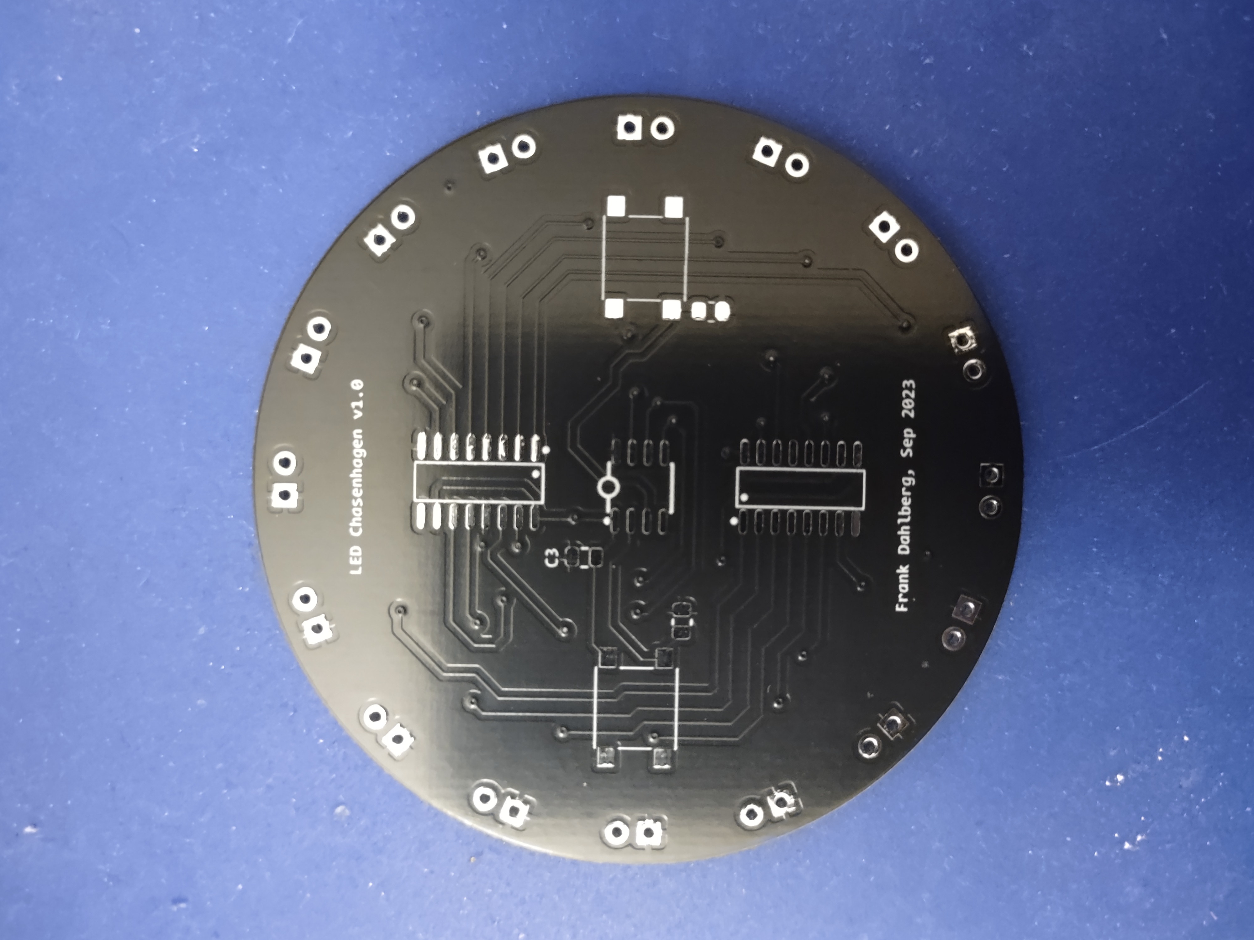
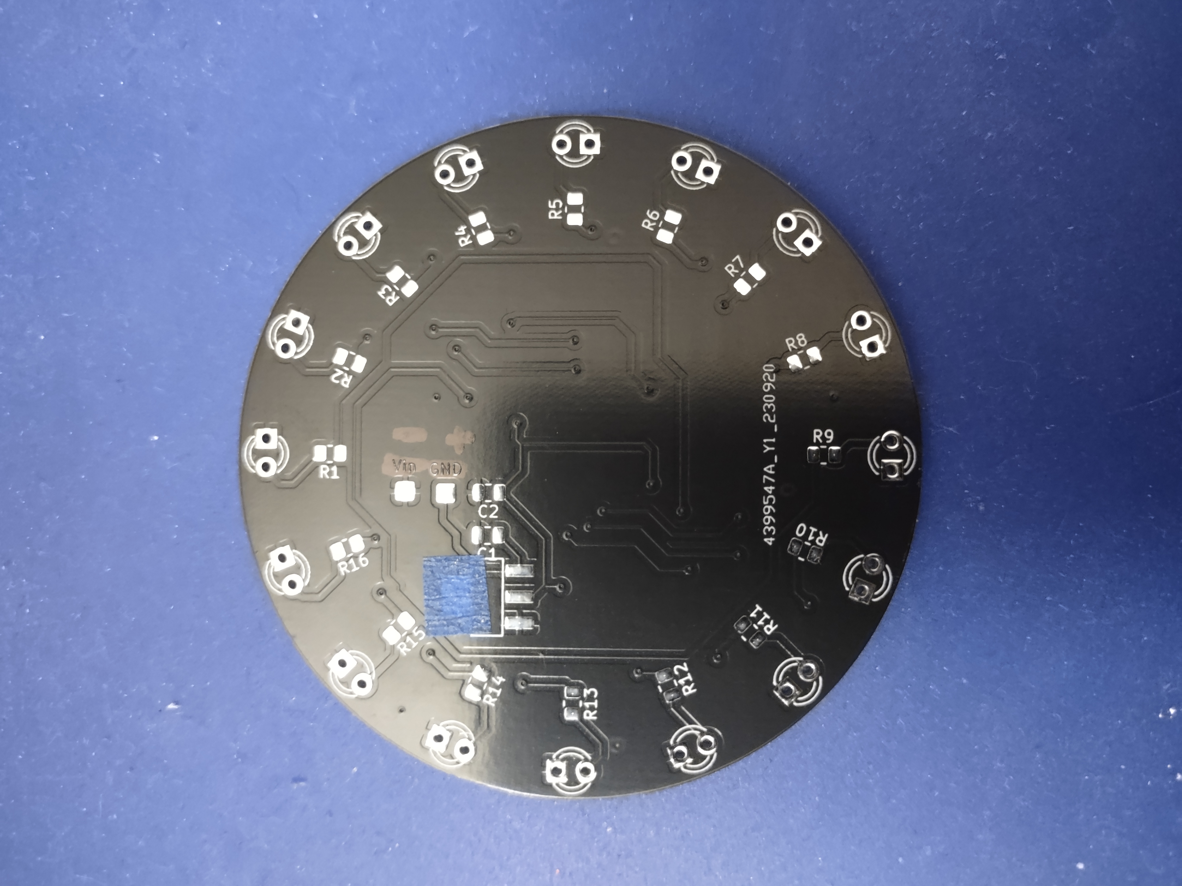
A couple of brief notes about this board, I had the boards produced at JLCPCB in China, and was very satisfied (honestly kinda shocked) at how cheap, quick, and effective their service is. That said, I’ve also used OSH Park in the past. OSH Parks service is good for sure, but they have small annoyances (if you want a color other than purple you’ll pay a premium, and they leave burrs on the edges of the board that aren’t a big problem but you have to sand them down) that caused me to try JLCPCB for this go around.
Now for the real reason I’m making this post. I made a LOT of errors when making this board, and I learned a ton. That was in fact the point of this project. But I’d like to be able to say I learned my lessons, so I want to detail them here.
Verify your design!
I really don’t have an excuse for this one so I figured I’d list it first. The power requirement for this board was supposed to be simplicity itself, I have two pads, labelled Vcc and GND with the idea being that the user inputs 7-12 volts across those pads where it is regulated by an onboard LDO into 5 volts. I silk screened the pads the wrong way. What should be ground is labelled Vcc, and what should be Vcc is labelled ground. What a mistake. I burned up a 5V LDO during construction when discovering this, but luckily that was all I burned up. When you’re in the gerber stage of a design, you really want to get the thing done and out the door to the fab, but you really need a step to sleep, take a nap, think on the design, review it again, and look for small, silly mistakes like this.
Verify your components!
This one has two parts. I didn’t have a lot of the necessary components for this build in the right package types when starting the design, but since I was ordering from JLCPCB I figured I’d order what I needed from their sister company LCSC. LCSC is kind of like the DigiKey or Mouser of China. It’s not a bad company, their search and filter functions are great, and I’ve found some good stuff on there in the past. For this I needed some 74HC595 shift registers in a SOP-16, surface mount package. I happened upon the 74HC595A by Shenzhen Fuman Electronics, and I bought a few hundred of them (they’re cheap and I’m already paying for postage, so why not). The datasheet was only in Chinese, but the part number was 74HC595 something, and my design isn’t very concerned with voltage tolerances, temperature requirements, etc, so I figured it’d be fine. Upon receiving these chips, I learned that it was not fine. While these have a part number of 74HC595, they actually couldn’t be more dissimilar to actual 74HC595 shift registers!
- They don’t have output enable or serial clear lines, those are just called out as NC on the data sheet
- They are OPEN DRAIN OUTPUT! In that they don’t even pull their lines high, they are basically reverse logic chips! I guess they’re useful perhaps (I did check and verify that they do work in their reverse logic), but these are totally opposite from any 74HC595!
Upon discovering this I ordered some different chips from Ebay that worked fine and I was able to complete the build. I guess the moral of that story is to always verify the datasheet completely! Not that their datasheet was particularly helpful with the fact that these chips were 180 degrees off from an actual 74HC595 shift register. Just be careful out there.
The second part of this has to do with the 5V LDO that I selected for this design. I had actually ordered a bunch of SMD 5V LDOs from LCSC before starting this, so I figured I’d use one of those. These worked fine and did exactly what they claimed to, but when designing the PCB I made a poor assumption that the fin of the LDO (what you’d normally solder to a heat sink or a copper pour) was connected to ground. I really don’t know why I assumed this. I’ve used other THT 7805 chips in the past where I guess that was the case, and so I assumed that was always the case. Where the fin was electrically connected is not called out in the devices datasheet, so I guess I subconciously ‘made a guess’. In actuality, on the LDO I selected, the fin is connected to the Vout line, so upon first hooking up the LDO I promptly dead shorted Vout and GND, let the magic smoke out and destroyed one. Luckily I soldered up that section of the board first, before anything else as a test, so that’s all I burned up and I just removed the LDO, found my problem, and fixed it. Still, it was a stupid assumption, especially when I had a reel of the things on hand and could have easily metered out the component and discovered my error ahead of time. If you feel like you’re making an assumption, DON’T!
Debug pads are not a suggestion!
Towards the end of the routing of this design, I felt VERY constrained by routing space. Indeed, the last few traces I was viaing in and out all over the place to get the runs where I needed them to go. With that in mind, I did not make debug pads for the MCU. I figured I’d just program it off board and not worry about the thought of me needing to program it again. This was a mistake, and I should have spent the extra time to figure out some debug pads for at least the /MCLR, CDAT, and CCLK lines for the MCU. I didn’t have any SOP-8 breakout boards when I was first assembling this (they’re on order), and I ended up doing some crazy soldering/wire hookup jazz to program it. It worked, but it took about half a day.
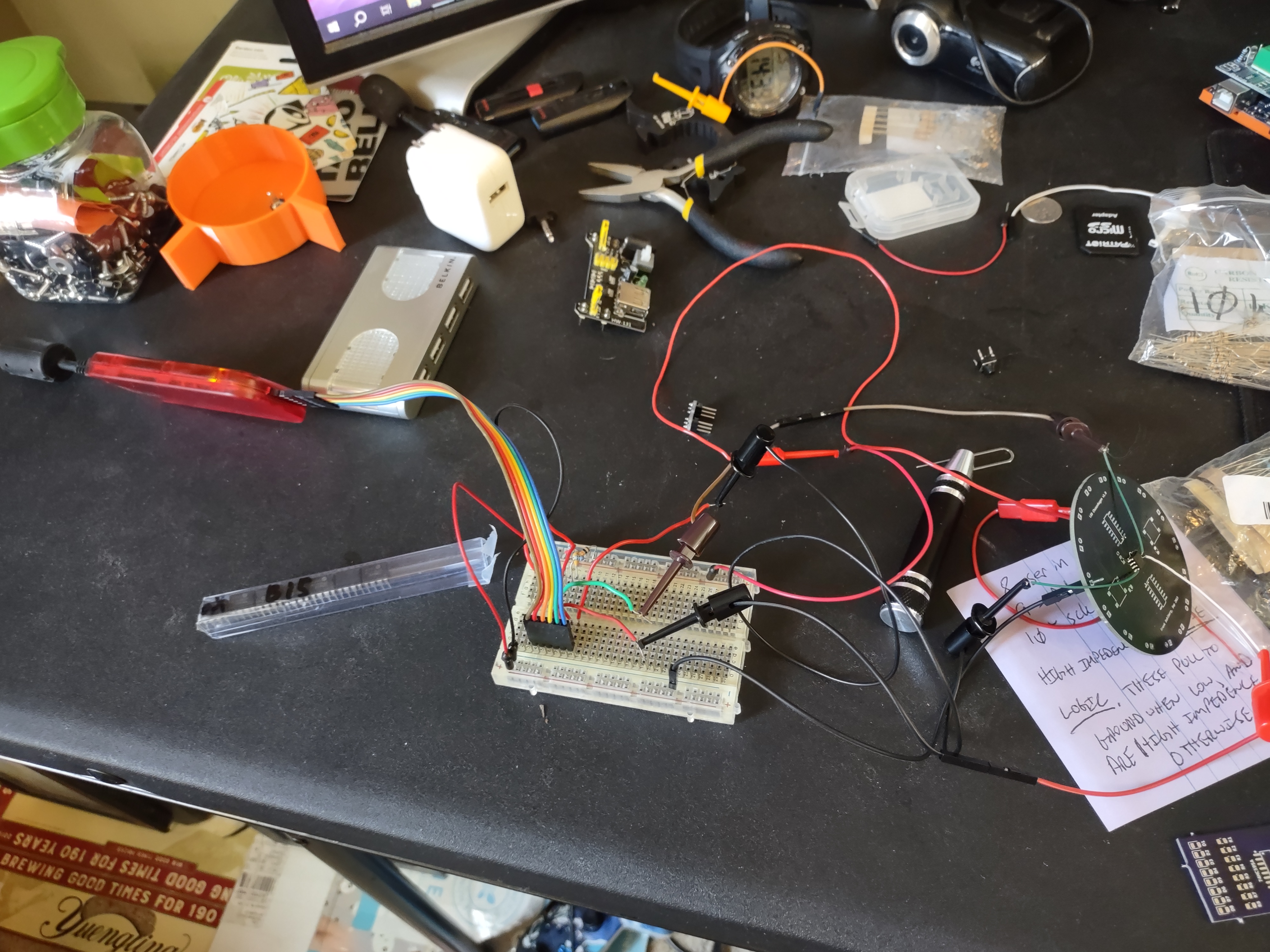
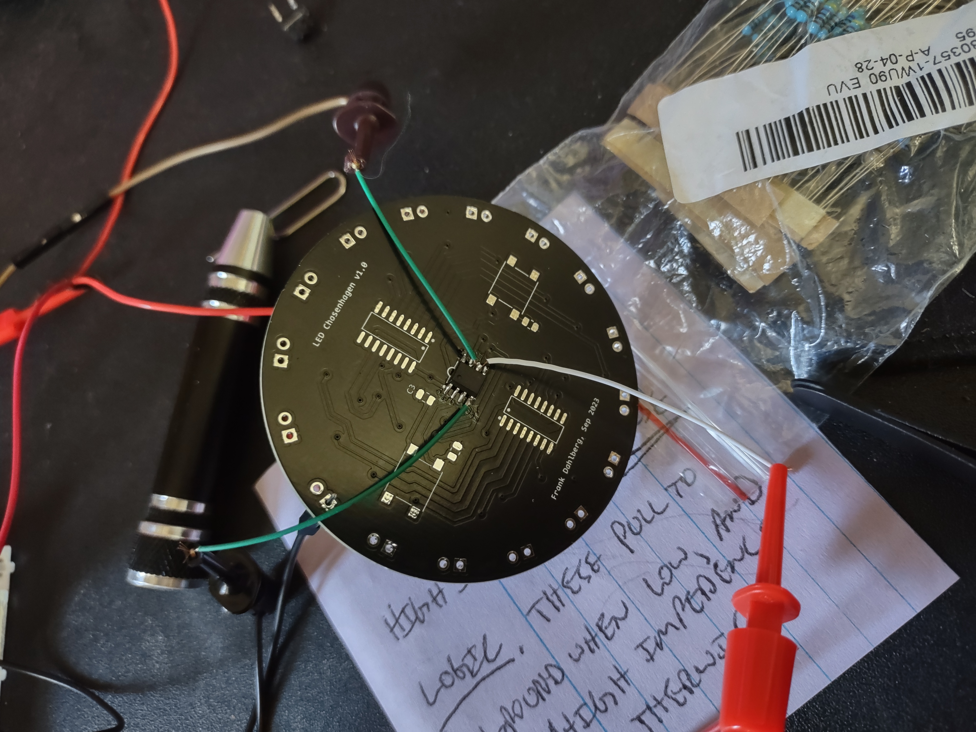
So I was fairly set in my general decisions for components for this build. I wanted to use 74HC595 shift registers, I wanted to use a PIC12F629 microcontroller, and I wanted to use 0805 passive components. For the ICs, I’d used those in the previous build and I knew that they interacted as designed and worked well (I didn’t want to rig up a whole other test and protoboard for a PCB design project). For the passives, the little bit of SMD solder work I’ve done in the past told me that I was confident with 0805 sized parts, and that I could solder them reliably. When I started the routing I thought ‘I’ll just put pads where they make sense’, and at the end of routing, nowhere made sense so I elected to not have them. This was a mistake, and any future PCBs should have these pads planned and positioned as critical components ahead of time. It’s fine if they’re not evently spaced, logically laid out, etc, but they absolutely have to happen. To be honest, I’m surprised I even got the chip programmed in it’s current state.
The PIC family, or at least my experience with the PIC family, is very finicky!
These are PIC12F629 MCU chips and the programmer I have is a ‘real’ from the factory Microchip PicKit2 programmer. This is a very old piece of tech (top of the line back in 2009 or so) so I don’t feel like I have the experience necessary to make an adequate assessment of Microchip’s current offerings. However, for their 2009 era offerings, I can say that things appeared to ‘just barely work’. The programmer continuously reported that it failed to see an MCU, until I plugged the programmer in with a painfully short USB cable, and that fixed that problem. Then I started running into an issue where the programmer would report that the OCSL calibration was bad, which I learned was fixed by unplugging and replugging the programmer, and the restarting the PicKit2 programming application. Finally, every now and then I got an error that the chip programming would fail at address 0x000000, which was also remedied by unplugging/replugging the programmer and restarting the application. Also I had to use the Windows based stand alone PicKit2 programming application (v2.61), as the MPLABx software doesn’t support that old programmer anymore. All of this to say that the setup is very flaky, and combined with my lack of debug pads, I was really crossing fingers to even get the chip programmed.
That’s about it for this project. It sounds like a lot written up like that, and honestly there were some pretty stupid assumptions and mistakes made along the way, but hey that was the whole point of this project. Even with all the problems described above, the board does in fact work! I truly can’t desribe how fun it is to conceptualize a (semi) complicated board, lay it out yourself, get it fabbed, solder it up, and then have that board actually work! I’m not sure what the next few steps of board design will be for me, but right now I hope to start laying out some more complicated multi layer boards, specifically with some MCUs and microprocessors on them, and get those working.
Thanks for reading!